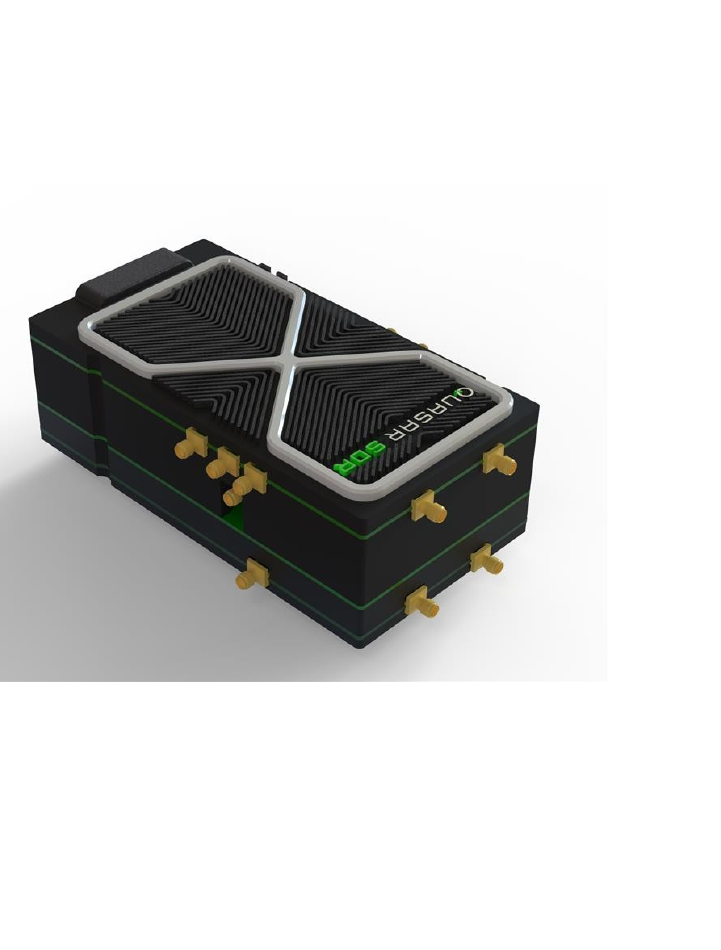
1
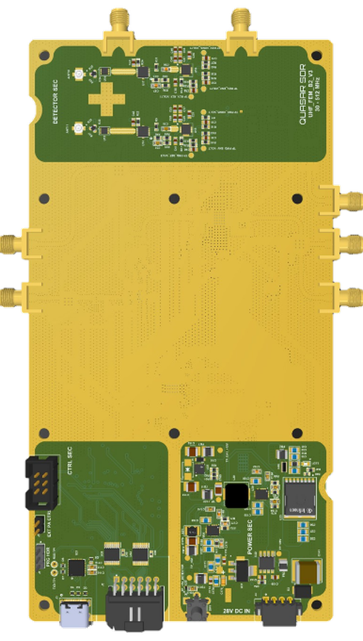
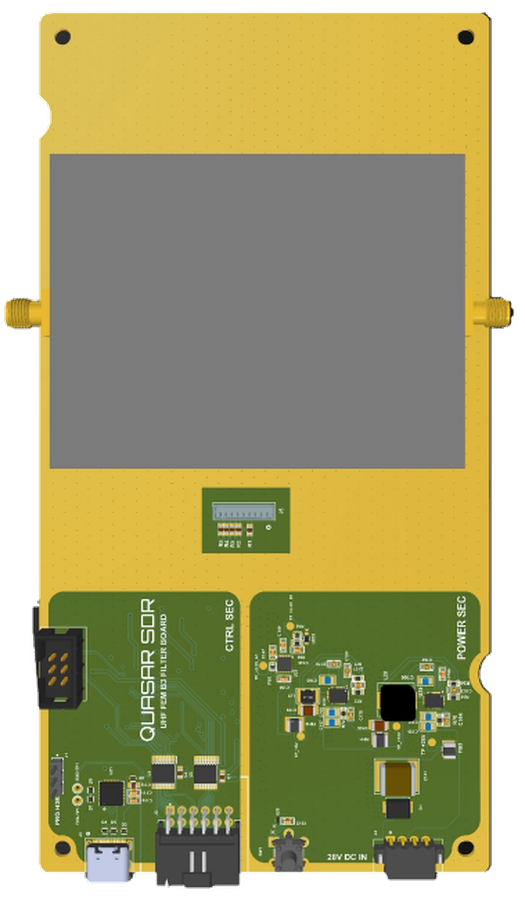
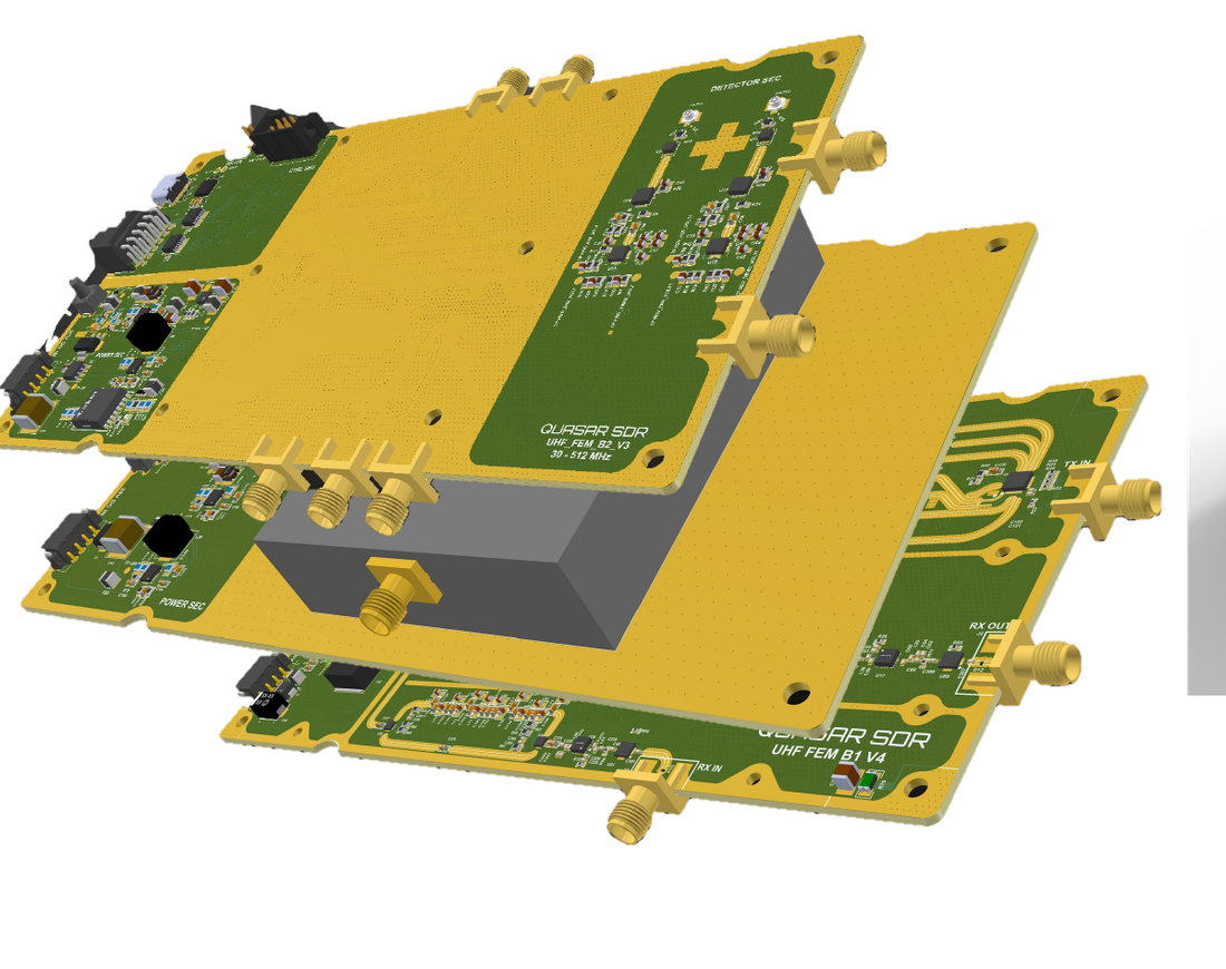
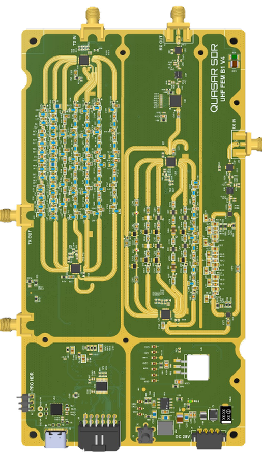
B1 — Filter Bank (SDR Side)
SDR-side Tx/Rx conditioning with switched BPF banks
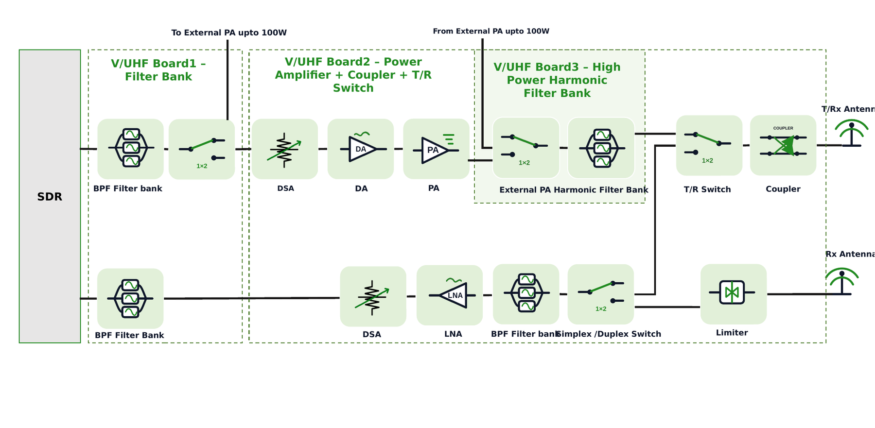
Front end on the SDR side: switched BPF filter bank, DSA, LNA, driver amplifier, simplex/duplex switch, and limiter. Cleans the SDR's Tx output and conditions Rx signals before the high-power stages. Seven BPF bands cover 30 to 590 MHz.
Key blocks
- BPF Filter Bank (Tx / Rx, 7 bands)
- Digital Step Attenuator
- LNA
- Driver Amplifier
- Simplex / Duplex Switch
- Limiter
QSR-VU-B1-OCopen card